歡迎您,浏覽新(xīn)港海岸(北(běi)京)科(kē)技有限公司(sī)官方網站!
服(fú)務(wù)熱線:+86-10-53821869 / +86-755-23480857
港海岸")
是描述信息")
NCS25D34
- 輸入類型 : LVPECL, LVDS, CML, SSTL, HSTL, HCSL, LVCMOS
- 輸入端口數(shù) : 3
- 輸出端口數(shù) : 4
- 輸出類型 : LVPECL, LVDS, HCSL, Hi-Z
- 器(qì)件(jiàn)類型 : Differential Buffer
- Core Supply Voltage(V) : 3.3V
- Output Supply Voltage(V) : 2.5V, 3.3V
- Output frequency(Min)(MHz) : -
- Output frequency(Max)(MHz) : 3100
- Additive Jitter(fs) : 43
- Temperature Range : -40 to 85
- Package : 32-pin QFN(5mm x 5mm)
輸入端口數(shù) : 3
輸出端口數(shù) : 4
輸出類型 : LVPECL, LVDS, HCSL, Hi-Z
器(qì)件(jiàn)類型 : Differential Buffer
所屬分類
Clock Buffer

NCS25D34
産品描述
産品描述
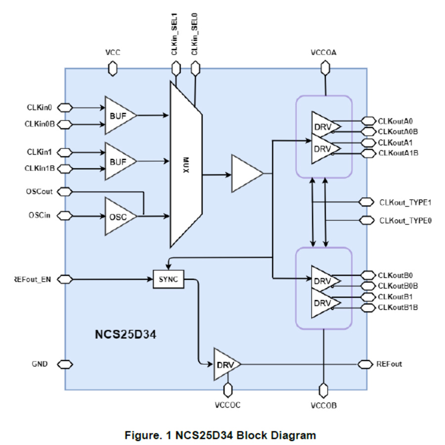
The NCS25D34 is a highly versatile, high-performance, 4-output differential fanout buffer and level translator which can operate up to 3.1GHz with ultra-low additive jitter.
The input clock can be selected from two universal differential or single-ended inputs, or one crystal input which can be overdriven by external single-ended clock. Crystal input frequencies from 8MHz to 50MHz are supported.
A 3:1 input MUX controlled by two external pins is implemented to distribute the selected input clock to two banks of 2 differential outputs and one LVCMOS reference output.
Both banks of differential outputs can be configured as LVPECL, LVDS, HCSL driver mode or disabled mode by two external pins.
The NCS25D34 operates from a 3.3V core supply and 3 independent 3.3V or 2.5V driver output supply, and does not have power supply sequencing requirements between the core and output supply domains.
産品參數(shù)
High-performance clock buffer with Ultra-low noise floor of -167 dBc/Hz
• Level translation from 3.3v core supply to output Supply of 3.3V or 2.5V
• 3:1 Input clock multiplexer which is selectable through input pins.
Two universal inputs operate up to 3.1GHz and can accept LVPECL, LVDS, CML, SSTL, HSTL, or HCSL signals
Both differential and single-ended input are supported
Support either DC or AC-coupled input interface
Crystal input frequencies from 8MHz to 50MHz
Crystal overdrive mode with input frequency up to 250MHz
• 4 differential output with two output supply banks
Support LVPECL, LVDS, HCSL or Hi-Z output mode
Ultra-low additive jitter (at 156.25MHz)
40 fs RMS (10K to 20MHz, LVPECL)
52 fs RMS (10K to 20MHz, LVDS)
• Highs PSRR (at 156.25 MHz)-67 dBc LVPECL, -79 dBc LVDS
• LVCMOS reference clock output with independent VCCOC supply and synchronous enable input
Core Supply Voltage(V):3.3V
Output Supply Voltage(V):2.5V, 3.3V
Output frequency(Min)(MHz):-
Output frequency(Max)(MHz):3100
Additive Jitter(fs):43
Temperature Range:-40 to 85
Package:32-pin QFN(5mm x 5mm)
關鍵詞:
集成電路(lù)
芯片
半導體
相關産品

産品咨詢
客戶留言
描述:

北(běi)京總公司(sī)
北(běi)京市(shì)朝陽區(qū)望京綠地(dì)中心A座A區(qū)9層
深圳子(zi)公司(sī)
↵廣東省深圳市(shì)福田區(qū)深南大道(dào)6019号金潤大廈8層
西安分公司(sī)
西安市(shì)高(gāo)新(xīn)區(qū)錦業一路(lù)52号寶德雲谷國際B座2003
合肥子(zi)公司(sī)
↵合肥市(shì)高(gāo)新(xīn)區(qū)創新(xīn)大道(dào)2800号創新(xīn)産業園2期F棟705
電話:+86-551-63657380